monolithic dual high-speed 16-bit D/A converter is described. In the binary weighted current network a dynamic current divider is used to obtain the required high accuracy of the six most significant bits without any adjustment proeedure or trimming techniqne. To construct the ten least significant bits a new approach is used to construct the passive divider stage based on emitter sealing of transistors. As the bk switches are optimized for fast-settling and low-glitch current, both converters can be used without extra sample-and-hold or degtitcher circuitry at sampling frequencies up to 200 kHz. The converter has a differential linearity of 0.5 LSIf over a temperature range of - 20 to +70C. The high linearity of the converter results in a dktortion of 0.001 percent over the audio band. The chip is processed in a standard bipolar process and the die size is 3.8 X 5.5 mmz
IEEE JOURNAL OF SOLID-STATE CIRCUITS, VOL. SC-21, NO. 3, JUNE 1986
HANS J. SCHOUWENAARS, EISE CAREL DIJKMANS, BEN M. J. KUP, AND ED J. M. VAN TUIJL
I. INTRODUCTION
In high-performance digital audio equipment such as Compact Disc players and digital tape or cassette recorders, the total dynamic behavior of the D/A conversion system plays a very important role. This imposes some strong demands on the D/A converter design such as oversampling capabilities and stereo-signal handling. Oversampling techniques allow digital filtering, which eliminates the need for high-order analog low-pass post-filtering. Phase distortion can affect the stereo information at the high-end of the audio band. Furthermore, oversampling increases the dynamic range of the converter which allows for a digital implementation of tone-control systems. A dualchannel D/A converter approach is used compared to a time-multiplexing system with an extra sample-and-hold function. The extra sample and hold must be applied to avoid phase differences between the two channels at high frequencies. Recently, several techniques were introduced to construct a monolithic high-resolution D/A converter; some of them require high-speed internal digital circuits that interfere with a four-times oversampling capability within an acceptable power dissipation [1]. Another technique uses laser trimming [2], sometimes combined with an increase in process complexity to obtain the required accuracy [3]. However, a low-cost, untrimmed, insensitive to element aging, binary weighted current D/A converter based on dynamic element matching has also been reported [4]. This principle combines passive division with a dynamic system to improve accuracy in a standard process. The principle requires only some noncritical external filter ing capacitors and is well suited to fit the demands for the D/A converter design. Moreover, the bit current switches can easily be optimized for fast settling with a low-glitch energy in such a way that both converters can be used without external sample-and-hold or deglitcher circuitry. In the new dual 16-bit D/A converter this dynamic element matching principle is used to obtain the required accuracy for the six most significant bits. In order to minimize the number of pins needed for the external capacitors, a rather unusual approach is used to construct the remaining ten binary weighted bit currents. The principle uses emitter scaling of transistors and is based on the basic statistical rule that the relative accuracy improves with the square root of the numbers involved, assuming an uncorrelated distribution between the transistor matching. Another important goal for the dual D/A converter was the design of a flexible serial data input format, which allows an easy interfacing between various digital signal processing devices, operating at different word lengths.
![Philips TDA1541 - A Monolithic Dual 16-Bit D/A Converter]()
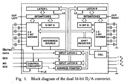
II. GENERAL CONVERTER DIAGRAM
Fig. 1 shows the block diagram with the most important parts of the dual 16-bit D/A converter and shows clearly the dual-channel approach. The reference current source that is common for the two identical converters is fed to three 2-bit dynamic divider stages which perform the required accuracy for the six most significant bits. One output current of the last dynamic divider is fed to the 10-bit passive divider. The 16-bit currents are switched to the output line of the D/A converter by the bit switches which are controlled by the data latches. To minimize timing errors the converter contains on-chip data latches. In order to obtain a low capacitive feedthrough the data input is in a serial mode which requires only four input pins. The digital inputs are TTL compatible and the circuit accepts two different data input formats. An internal emitter-coupled oscillator supplies the dynamic divider stages with the necessary control signals. In the internal digital part a low-voltage swing unsaturated current-mode logic (CML) is used for speed and low-interference noise.
III. THE REFERENCE CURRENT SOURCE
The low-noise reference current source Iref is based on the bandgap of silicon and shows the wellkknown parabolic temperature behavior. With integrated current setting resistors a temperature coefficient of 200 ppm/ºC can beobtained. However, in digital audio applications the dc stability of the reference source is not that important since this temperature depefidence only leads to 0.2-dB gain variation of the output current over a temperature range of 100ºC.
![Philips TDA1541 - A Monolithic Dual 16-Bit D/A Converter]()
![Philips TDA1541 - A Monolithic Dual 16-Bit D/A Converter]()
IV. THE BINARY WEIGHTED CURRENT NETWORK
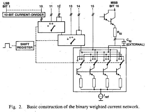
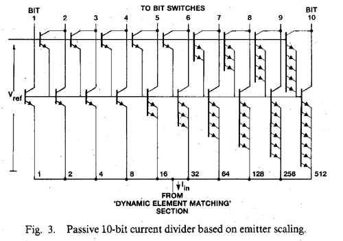
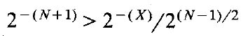
When high sampling rates are required, the binary weighte& currents principle offers the best possibilities to construct a high-performance D/A converter. However, in high-resolution converters this principle sets a high demand on the relative accuracy of the bit currents. To obtain the required accuracy of the six most significant binary weighted bit currents, dynamic element matching is used. Fig. 2 shows the basic construction Of the binary weighted current network of the dual D/A converter. The reference current is divided into four nearly equal parts by means of a passive current divider using resistor matching. The four currents are interchanged during equal time intervals controlled by an internal shift register. The output currents of this dynamic divider stage alll have the same average value with a relative error which ecluals the resistor matching accuracy times the timing accuracy of the interchanging network. The required weighting accuracy between the two MSB currents in a 16-bit D/A converter of 0.5 LSB can easily be obtained. A more complete description of dynamic current division is provided in [4]. Two of these interchanged currents are added to construct the most significant bit current. The third one is fed directly to the bit switches, while the fourth current flows through a second identical dynamic stage. Three of these dynamic divider stages are needed to construct the six MSB currents. The interchanging network consists of Darlington differential pairs which are optimized for base current losses and interchanging frequency. The clock frequency of the interchanging shift register is not related to the sample frequency and is generated by a free-running emitter-ccnpled oscillator which operates at about 250 kHz without affecting the accuracy. A simple low-pass filter is used to remove the ripple of the bit currents due to the interchanging operation to obtain the accuracy and is only drawn here for the MSB. This approach requires seven noncritical external ceramic cttpacitors for each channel. Furthermore, the thermal noise on the bit currents is reduced by the filtering operation down to 120 dB below the maximum output level of the converter. The Darlington stages isolate the filter operation from switching transients of the bit switches. One output current of the last dynaniic divider is fed to the new 10-bit passive divider. Fig. 3 shows the basic concept of the passive current divider based on emitter scaling of transistors. This concept is used for the remaining ten least significant bits. It only consists of 1024 Darlington transistors and does not require any trimming or adjustment procedure and operates over a large temperature range. As all transistors have the same base–emitter voltage, they all have equal collector currents. In this way the input current Iin is divided into 1024 equal currents with a value of one LSB. The output current of the MSB bit of this passive divider is constructed by a combination of 512 collector currents. The required accuracy can only be obtained by carefully randomizing the transistors over the passive current divider surface to eliminate temperature gradients and to minimize mask errors. Assuming a Gaussian distribution between the offset voltages of the transistors, the relative accuracy of the coflector current improves, according to statistics, with the square root of the number of transistor pairs involved. In an N-bit passive current divider the required accuracy is given by
![Philips TDA1541 - A Monolithic Dual 16-Bit D/A Converter]()
in which
2
-(N+l)
- the required relative accuracy between two binary weighted output currents ( = 0.5 LSB);
2
-(x)
- the attainable relative accuracy between two single collector currents; and
2
(N-1)/2
- the square root of the number of transistors pairs incorporated in the scaling network.
In a 10-bit binary current network the required accuracy between the two MSB currents has to be < 0.5x 10⁻³. Since the scaling network consists of 512 transistors pairs, the relative error between the collector currents of a single transistor pair has to be <1.1 percent and this implies an offset voltage of 275 µV.
V. THE BIT SWITCHES
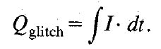
The bit switches are optimized for fast-settling and lowglitch current to avoid the need of extra sample-and-hold or deglitcher circuitry. Due to offset-binary coding, the largest glitch occurs at the zero crossing of the analog output signal. The charge of one glitch is given by the expression
The frequency dependence of the glitch current is now given by
![Philips TDA1541 - A Monolithic Dual 16-Bit D/A Converter]()
To switch the binary weighted currents to the output line of the D/A converter, three different types of switches are used depending on the value of the bit currents to be switched. To avoid differences in base current losses owing to the different bit currents, the six most significant bits are switched with a fast diode-transistor switch, as is shown in Fig. 4. The diode-transistor switch is controlled by data latches and driven by a differential amplifier. At the emitter node of the switch a voltage swing of half the collector swing is present. To avoid long settling times due to the parasitic load Zout, a cascode stage is added. To further minimize this parasitic load and to preserve the current generation network from switching transients, an extra cascode stage is added.
The next four bit currents are switched with compensated diode-transistor switches, as shown in Fig. 5. This compensation is added to cancel the voltage swing at the current source connection which causes long settling times as these bit currents are small to discharge the parasitic capacitors. When the bit current is drained to Vref, an extra current Icomp is added to the current source connection and this causes an extra voltage drop over the resistor R, which cancels the voltage swing at the emitter node. Furthermore, a cascode stage is added to minimize the influence of the remaining voltage swing across the parasitic load, which is mainly the collector–substrate capacitance of the passive divider.
![Philips TDA1541 - A Monolithic Dual 16-Bit D/A Converter]()
During switching transients a small amount of compensation current flows into the output line of the converter. An error in the bit current could be introduced depending on the magnitude of the compensation current and the time duration of the current transient. The charge contribution of this current transient can be compared with the charge contribution of one LSB current during one sample period
The compensation current in the bit switch has about the same magnitude as the bit current itself. For bit number N the current Icomp can be written as
![Philips TDA1541 - A Monolithic Dual 16-Bit D/A Converter]() Figure 5
Figure 5
Assuming a charge error contribution <0.5 LSB this results in
![Philips TDA1541 - A Monolithic Dual 16-Bit D/A Converter]() Figure 6
Figure 6
For a sampling period of 5 µs and a transient time of 5 ns this compensation method can be used up to the tenth bit. To avoid large glitches in the output current this switching method is not used for the six most significant bits. The six least significant bits are switched to the output line with differential pairs, which are compensated for base current losses. For proper switching of the bit switches it is required to keep the output line of the D/A converter at a well-determined level. Normally an operational amplifier will be applied for this purpose. At the same time this operational amplifier can be used in an active high-order filter network as the output of the D/A converter has to be band-limited to attenuate out-of-band signals dow,l to a sufficiently low level to avoid intermodulati.on distortion in audio amplifiers and recorders.
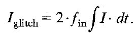
VI. INPUT FORMATS
To allow an easy interfacing between various digital signal processing devices operating at different word lengths, two different data input formats can be used. Fig. 6 shows the first input data format which is based on the Inter IC Signal (IIS) standard, in which the two input channels are time multiplexed. This standard provides an easy interfacing between digital signal processing devices, operating at various word lengths. In this standard three signals are used. The first one is the DATA signal. It consists of a sample of the right channell followed by a sample of the left channel. Any bit length is allowed although the MSB must be the first one. The second one is the BIT CLOCK signal. It is not only used to clock the DATA bits into the input latches, but also to determine exactly the moment at which the sample value appears at the output. The third one is the WORD SELECT signal, which directs the data bits to the left or right channel input latch. A new sampling period starts at the negative slope of the WORD SELECT signal.
![Philips TDA1541 - A Monolithic Dual 16-Bit D/A Converter]() Figure 7
Figure 7
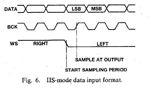
Fig. 7 shows the second possible input data format. In this mode the DATA signals of the left and right channel are applied simultaneously to two different input pins. Only one bit clock signal is used to clock both data signals into the converter. The positive slope of the latch enable signal is used to indicate the end of the data input action and to determine the moment at which the outputs change their sample values. This input format is especially suited for those cases in whi;h the circuits in front of the DAC use a nonstandard serial format.
VII. PRACTICAL D/A CONVERTER CHIP
Fig. 8 shows a photograph of the dual 16-bit converter. The circuit is processed in a standard bipolar technology with double-sided isolation and double-layer interconnection. The dual D/A converter needs a chip area of 3.8 X 5.5 mm² and is mounted in a 28-pin dual-in-line plastic package.
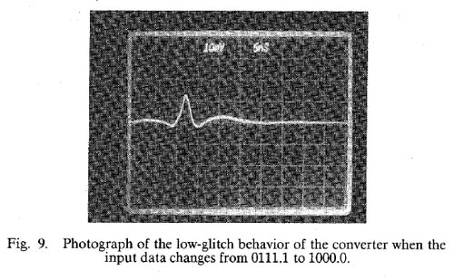
![Philips TDA1541 - A Monolithic Dual 16-Bit D/A Converter]() Figure 9
Figure 9
VIII. MEASUREMENTS
Fig. 9 shows a photograph of the most difficult bit transition (from O111.1 to 1000.0) where the largest glitch occurs. The output current of the converter is directly fed into the 50-ohm 1-GHz CRT input. Total glitch charge is within 0.4 pC. The contribution of the glitch current to the output current of the D/A converter is 0.25 ILSB (fin = 19 kHz, ILSB = 62 nA) and thus eliminates the need of extra deglitcher circuitry.
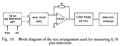
![Philips TDA1541 - A Monolithic Dual 16-Bit D/A Converter]() Figure 10
Figure 10
Fig. 10 shows a block diagram of the test arrangement used for measuring signal-to-noise ratio and total harmonic distortion. A true 16-bit digitally generated sine wave is applied to the data input of the dual D/A converter. The feedback resistor of the operational amplifier converts the output current of the converter into a voltage and a low-pass output levels. filter is used to attenuate out-of-band signals. A HP 339A measurement set is used for the measurement of signal-to-noise and total harmonic distortion. The sine-wave generator uses 64K samples of a full-scale sine wave stored in PROM’S. An address generator selects the succeeding samples, depending on the desired frequency, in such a way that the quantizing error has no correlation with the sine wave. A 13th-order symmetrical filter with O.1-dB ripple in the 20-kHz passband and 110-dB stopband attenuation above 23 kHz is used for the analog low-pass measuring filter. Furthermore, the filter must have a sufficiently low distortion to avoid that measurement results are being affected.
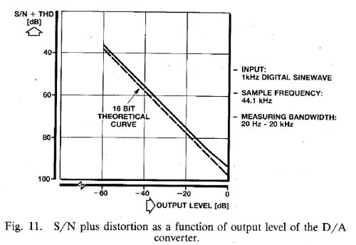
![Philips TDA1541 - A Monolithic Dual 16-Bit D/A Converter]() Figure 11
Figure 11
Fig. 11 shows the signal-to-noise ratio plus total harmonic distortion as a function of the signal output level of the D/A converter. The sample frequency is 44.1 kHz and the measuring bandwidth is 20 kHz. At full scale hardly any decrease in signal-to-noise ratio with respect to the 16-bit theoretical curve is found.
Fig. 12 shows the signal-to-noise ratio plus the total harmonic distortion as a function of frequency at different output levels. The converter is used four times oversampled with a sample frequency of 176.4 kHz. Measuring bandwidth is 20 kHz. At full scale a signal-to-noise ratio plus THD of 95 dB over the input frequency range can be obtained. At –20 dB a signal-to-noise ratio of more than 80 dB is measured. This means a dynamic range of over 100 dB.
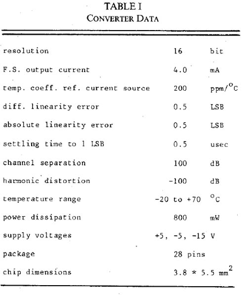
![Philips TDA1541 - A Monolithic Dual 16-Bit D/A Converter]() Table I gives some additional data of the dual 16-bit D/A converter.
Table I gives some additional data of the dual 16-bit D/A converter.
IX. CONCLUSION
A low-cost untrimmed dual 16-bit D/A converter has been realized in a standard bipolar process using a 6-bit dynamic divider and a 10-bit passive divider to construct the binary weighted current network. The combination of the high linearity and the low distortion with the very flexible input format makes the converter very attractive for application in high-performance digital audio equipment such as compact disc players ancl digital tape or cassette recorders. The very low thermal output noise at 120 dB below rhaximum output level and the fast settling of the bit currents allows the use of oversampling and noise shaping techniques to extend the dynamic range of the converter.